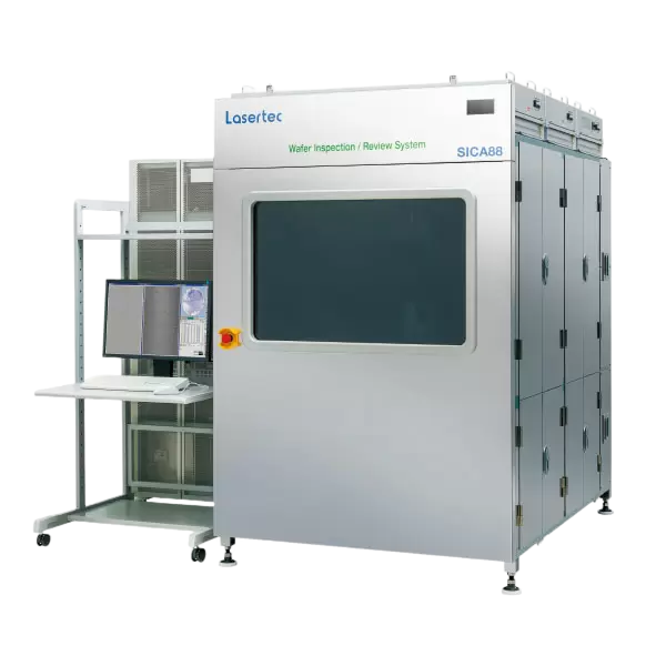
SICA88
Features
Concurrent inspection of various surface defects and Epi layer BPD/SF
High‑accuracy ADC enabled by ultra‑high‑resolution review images
High throughput (10 WPH with 6‑inch wafer)
Applications
Incoming and outgoing inspection of bare SiC wafers and SiC Epi wafers
Monitoring of SiC polishing and epitaxial growth processes
Management of SiC device manufacturing processes
SiC power devices are already used in air conditioners, photovoltaic systems, and railway vehicles, and their adoption in EVs is expected to accelerate, steadily expanding the market. However, due to manufacturing complexity, various issues such as crystal defects still occur in production, posing major challenges in both quality assurance and cost. Wafer manufacturers require improved quality and quality control of wafers, while device manufacturers seek higher yield and further cost reduction.
SICA88 combines surface inspection using confocal‑DIC optics with PL inspection on a single platform. Surface inspection detects scratches and epi defects on the wafer surface, while PL inspection simultaneously detects and accurately classifies defects such as basal plane dislocations (BPD) and stacking faults (SF) in the epi layer. Throughput is doubled compared with the previous SICA6X, and BPD inspection can be performed without sacrificing throughput. The system serves as a process monitor for wafer, epi, and device processes to identify root causes of defects, and enables process cost reduction through wafer grading and improved device yield.