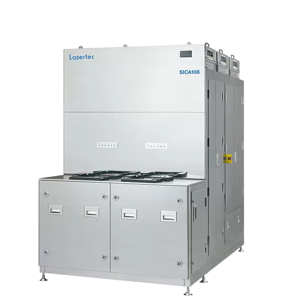
SICA108
Features
Concurrent inspection of surface defects and BPD/SF at high speed and with high sensitivity
Detailed classification of various defect types using high‑accuracy ADC and high‑resolution review images
Compatible with various automation systems, including AGV and OHT
Applications
Incoming/outgoing inspection of SiC wafers and epi wafers
Monitoring of SiC epitaxial growth process
Monitoring of SiC polishing process
Management of SiC device manufacturing processes

SiC power devices are increasingly adopted in EVs, air conditioners, photovoltaic systems, and railway vehicles, contributing to a decarbonized society. However, due to the difficulty of wafer manufacturing processes, numerous defects still impact yield during production, making stable mass production of high‑quality wafers and cost reduction major challenges.
To address these challenges, we developed SICA108. Building on the industry‑standard SICA88, SICA108 features renewed inspection optics to further boost throughput and improve SiC wafer quality assessment and cost of ownership (COO). As with the predecessor, surface inspection detects scratches, crystal defects, and particles on the wafer surface, while PL inspection simultaneously and sensitively detects basal plane dislocations (BPD) and stacking faults (SF) in the epi layer. It also offers high‑accuracy defect classification and judgment using Lasertec’s proprietary deep‑learning technology, enabling early detection and analysis of defects that cause device failures. In addition, it supports factory automation such as AGV/OHT used in smart fabs.