MATRICS X810EX Series
Features
Supports design nodes 20nm~7nm and beyond
High-power 213nm QCW laser (>400mW), 2x conventional power
Scan time: 38 minutes per 100mm×100mm area
Pattern dimension distribution (CD uniformity) measurement and visualization function
Supports photomask RSP150 and RSP200
Fully automated inspection possible with OHT (Overhead Hoist Transport) integration
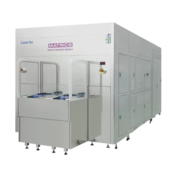
Integrated design of stage system and electrical rack system achieves compact footprint
Applications
Acceptance inspection and regular quality assurance inspection of photomasks at wafer fabs
Pre-shipping inspection in photomask manufacturing processes
Specifications
| Inspection Mode | Multi-die mode, Single-die mode |
| Inspection Scan Time | 38 minutes per 100mm×100mm area |
| Supported Mask Types | Cr, MoSi, OMOG |
| Mask Size | 6 inches |
The MATRICS X810EX series is a semiconductor mask inspection equipment supporting design nodes 20nm~7nm. It is a semiconductor mask inspection system that achieves high sensitivity, high speed, and low CoO, supporting design nodes 20nm~7nm and beyond.
Equipped with a high-power 213nm QCW laser (>400mW) with 2x conventional power, it achieves even higher sensitivity. Through high-speed defect detection system, the scan time is 38 minutes per 100mm×100mm area.
It is equipped with a function to measure and visualize mask pattern dimension distribution (CD uniformity) simultaneously with mask inspection. It supports photomask RSP150 and RSP200, and fully automated inspection is possible with OHT (Overhead Hoist Transport) integration.