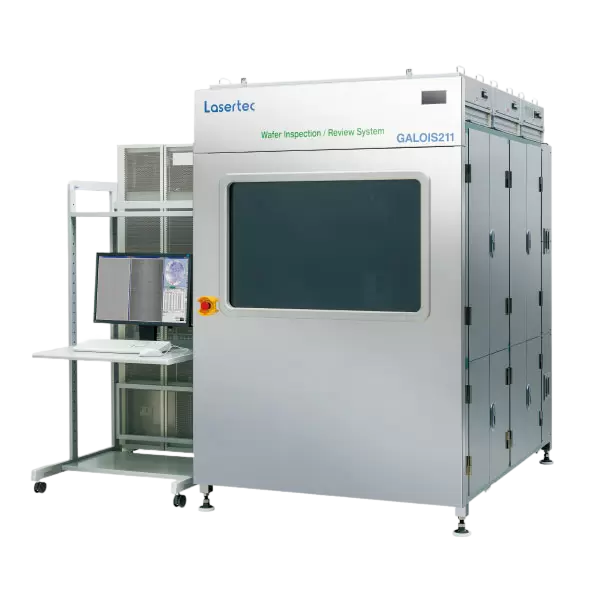
GALOIS211
Features
Confocal optics - best suited for transparent wafer inspection - eliminates the effect of noise from the backside of the wafer
Differential interferometry captures shallow-scratch and various crystallographic defects with high sensitivity
Wavelength selection by light source and optical filters enables the inspection of wafers with GaN-on-SiC or other hetero-epi structures under optimal conditions, unaffected by thin-film interference
Advanced image processing technology enables inspection which is unaffected by GaN surface morphology
High-speed inspection at 6 minutes per 6-inch wafer extends use to the production phase
Defect mapping, defect classification, and marking functions support defect analysis
Applications
Bulk GaN wafer inspection
GaN epitaxial layer (homo-epi and hetero-epi) inspection
Analysis of changes in defect characteristics before and after heat processing in the device making process
Management of the epitaxy process and processing tools
Management of grinding material development and grinding processes
Specifications
| Dimensions | 3,052mm (D) x 3,250mm (W) x 1.990mm (H) Including maintenance space |
| Wafer size | Up to φ8 inches |
| Applicable wafer types | Bulk GaN, homo-epi and hetero-epi GaN wafers |
| Inspection time | 6 minutes per wafer (φ6 inch wafer, with 10x lens) |
GALOIS211 enables faster detection and high‑resolution review of various defects on GaN wafers.
With bright‑field confocal optics, the GALOIS series provides high‑speed detection and high‑resolution review imaging for GaN wafer defects as an inspection/review system.
With the global shift toward energy saving, the need for technologies that maximize energy efficiency is rising. Wide‑bandgap semiconductors such as SiC and GaN are expected to play a key role in power electronics, high‑speed communications, and LEDs, driving R&D for quality improvement and cost reduction. While SiC is already moving toward mass production (our SICA88 inspection/review system is widely recognized as an industry standard for its high throughput, accurate defect classification, and high‑resolution review images), the spread of GaN devices is still challenged by wafer manufacturing costs and numerous crystal/process defects, requiring continuous wafer quality improvement. To address these issues, Lasertec developed the GALOIS series to sensitively and rapidly detect/classify process and crystal defects and provide high‑resolution defect review.
Combining our core confocal and differential interference (DIC) optics with state‑of‑the‑art image processing, GALOIS detects various defects on GaN wafer surfaces with high sensitivity while being robust to backside reflections from transparent substrates and surface morphology. Defect classification leverages high‑performance computing and machine‑learning models including deep learning, enabling accurate classification of irregular‑shaped defects based on high‑resolution review images, concurrently with inspection. All full‑wafer review images are stored for later analysis of unknown defects. High throughput is achieved (6‑inch wafer in 6 minutes), making the system applicable to future mass‑production lines. GALOIS is effective not only for outgoing/incoming inspections of GaN wafers but also as a process monitor for wafer/epi/device processes, helping identify root causes of defects and improve yield.