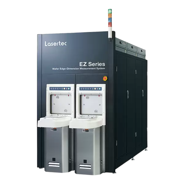
Wafer Edge-Dimension Measurement System
EZ Series
For wafer edge yield management and process error analysis
Features
Defect inspection using high contrast images from confocal optics
Automatic defect classification including pit/bump analysis by proprietary algorithm
High-resolution 3D measurement that facilitates defect type identification and estimation
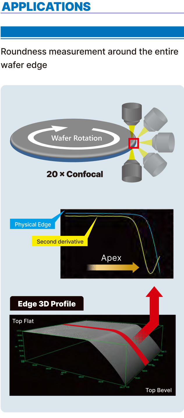
Applications
Quantitative management of wafer edges for in-line QC and early warning of process errors
Follow-on analysis of chip defects at wafer edges using SPC
Root cause analysis of yield loss at wafer edges