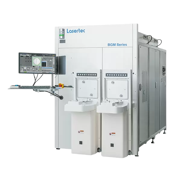
BGM Series
Features
TSV depth measurements based on a combination of Lasertec-proprietary interferometer and IR optics
Applicable to measurements in both pre- and post-back grinding processes
BGM300 provides an optimum solution for back grinding process

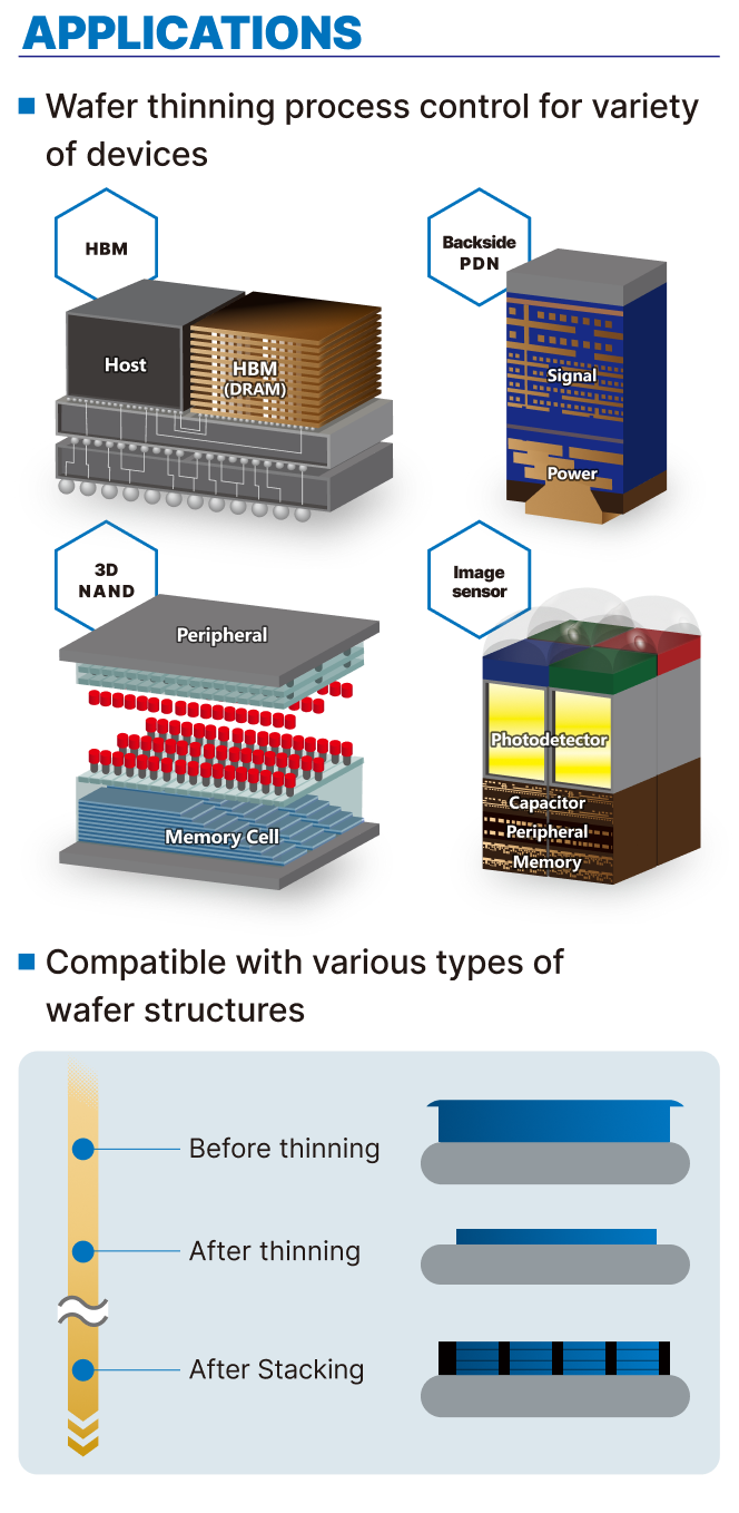
Applications
Silicon thickness and TSV depth measurement prior to the back-grinding of TSV wafers
Remaining silicon thickness (RST) measurement after the back-grinding of TSV wafers
Detection of abnormal adhesive thickness of bonded wafers
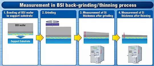
Silicon thickness measurement after the back-grinding/thinning of BSI wafers
Specifications
| Dimensions (mm) | 1,450mm(W) x 2,650mm(D) x 1,885mm(H) |
| Applicable wafer size | 300 mm wafer |
| Applicable wafer type | Bonded TSV or BSI wafers |
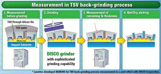
In pursuit of further high density, high-speed operation, and low power consumption of semiconductor devices, three-dimensional stacked devices that build circuits vertically by stacking chips are being put into practical use. Each chip is connected vertically by through-silicon vias (TSV: Through Silicon Via).
BGM300 rapidly measures Si thickness and TSV depth before the grinding process to prevent Cu contamination and enable optimal grinding. It also enables measurement of the remaining Si thickness at the Via portion after grinding.