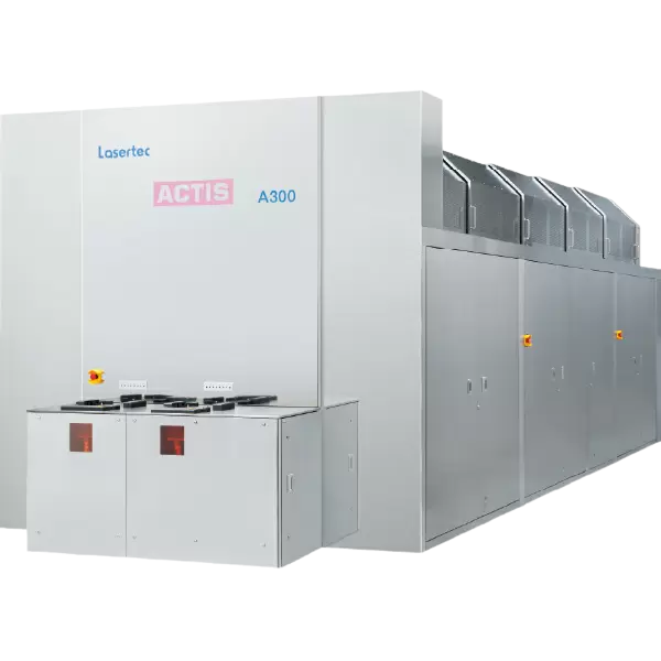
ACTIS A300 Series
Features
Supports defect inspection of EUV masks for High NA lithography
Supports defect inspection of EUV masks for current NA lithography
High productivity achieved through efficient optical design and adoption of "URASHIMA" light source
Applications
Defect inspection in EUV mask manufacturing processes
Acceptance inspection of EUV masks in wafer fabs and periodic quality confirmation inspections
To pursue higher functionality, improved operating speed, and reduced power consumption of semiconductor devices, miniaturization continues to be required in their manufacturing processes. Semiconductor manufacturing using EUV lithography is already being applied to mass production, and our EUV pattern mask inspection equipment ACTIS A150 has received high praise in the market for its excellent inspection performance.
We have commercialized ACTIS's next-generation model, the A300 series, to respond to further miniaturization processes and High NA EUV lithography.
The A300 series adopts newly designed optical systems and the high-brightness light source "URASHIMA," achieving significantly higher defect detection performance compared to the conventional A150 series.
High NA lithography employs an anamorphic optical system with different projection magnifications in the X and Y directions, requiring different resolutions in each direction. The A300 series supports EUV mask inspection for both current NA lithography and High NA lithography.