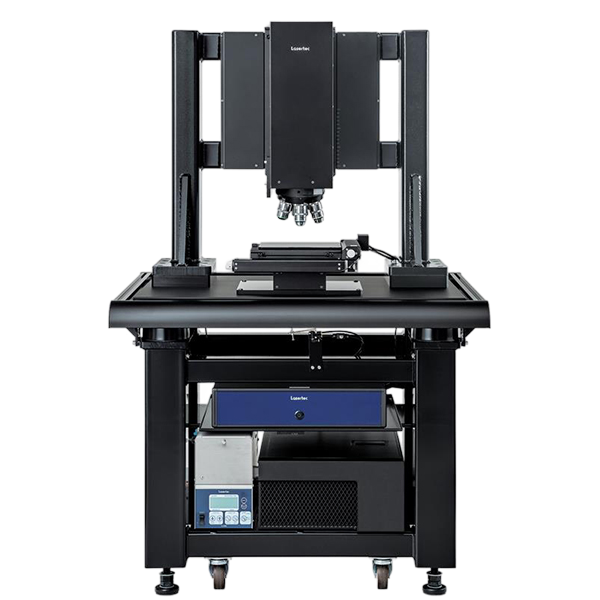
OPTELICS IR
Effective for internal observation of devices using materials that transmit IR, starting with silicon wafers. Particularly suitable for research and development and process improvement applications in the rapidly growing advanced packaging market, such as alignment deviation measurement, void inspection, and observation of adhesive delamination.
Features
High-brightness IR confocal optical system
High-resolution observation at wavelengths of 1000-1500nm
High-precision XY measurement
Height measurement through optical sectioning in the Z-axis direction
Applications
Transmissive internal observation of materials with IR transmission properties, such as silicon wafers
3D packaging evaluation and inspection
Internal defect analysis of advanced packaging devices
Non-destructive measurement of etching amount for sacrificial layer etching of oxide films
Measurement of bonding misalignment
SOI active layer thickness measurement