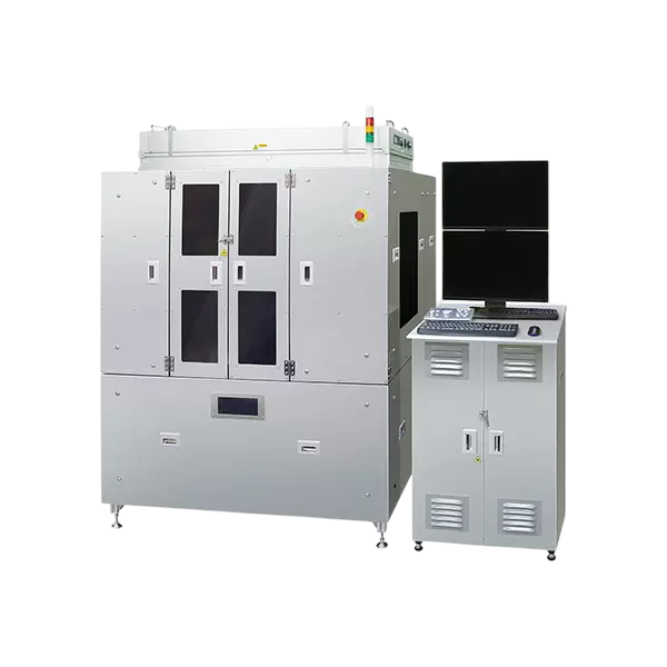
OPTELICS AI²
The semiconductor device market continues to see growing demand in various fields such as power devices, 5G, and HPC, and semiconductor device manufacturing processes require continuous product development for performance improvement. Commercializing devices using new designs and new materials requires solving numerous cross-departmental challenges, including prototype evaluation, quality control during mass production, and process improvement for yield enhancement.
"AI²" is capable of handling everything from automatic defect inspection to defect review and 3D shape measurement in a single system, making it useful in all scenarios from development to production.
This system integrates our core technology of confocal optical systems, automatic inspection software developed through semiconductor inspection equipment development, and newly designed high-speed hardware to achieve both high-throughput high-speed inspection functions and high-magnification shape measurement functions using confocal microscopy. In addition, AI inspection technology using Deep Learning provides advanced inspection functions such as high-precision image classification, patterned substrate inspection, and extraction of specific types of defects.
Features
Handles everything from automatic defect inspection to defect review and 3D shape measurement in a single system
High-magnification shape measurement function using confocal optical system
AI inspection technology using Deep Learning
High-precision image classification function
Patterned substrate inspection capability
Specific defect type extraction function
Applications
Semiconductor device prototype evaluation
Quality control during mass production
Process improvement for yield enhancement
Inspection of power devices, 5G, and HPC-related devices
Evaluation of new design and new material devices